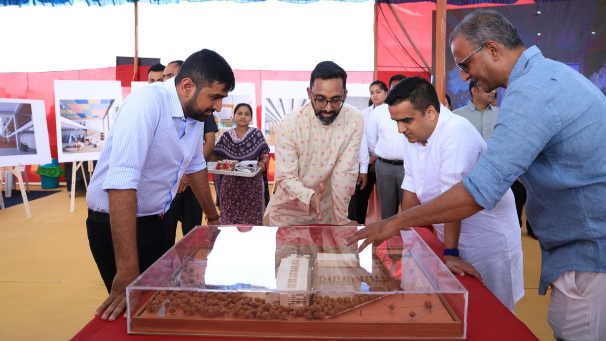

In a pivotal move to strengthen India’s semiconductor ecosystem, the Union Minister for Electronics and Information Technology, Ashwini Vaishnaw, has approved the establishment of the NaMo Semiconductor Laboratory in IIT Bhubaneswar. Funded through the MPLAD Scheme at an estimated cost of Rs. 4.95 crores lab is intended to develop indigenous talent in chip manufacture and packaging, thereby strengthening India’s ambition of becoming self-reliant in the semiconductor sector.
Creating Industry Ready Talent for Bharat
The new facility shall be the key skill development hub to equip Indian youth with state-of-art skills tailored to the semiconductor industry. According to official sources, the NaMo Semiconductor Lab will act as a talent incubator that will transform IIT Bhubaneswar into a top-tier institute in semiconductor research and hands-on education. This initiative shall align with the country’s larger vision for creating a robust workforce that will support upcoming chip manufacturing and packaging plants across the country.
ALSO READ: ChatGPT Gets Smarter: Use Spotify, Figma, Canva & More Without Leaving the Chat
Enhancing the ‘Make in India’ & Design Missions
Largely linking to the preceding initiatives, this project will also help hasten innovation and indigenous manufacturing of semiconductor technologies in India. To this day, India commands about 20% of the world’s chip design talent, with students using the latest Electronic Design Automation (EDA) tools in almost 300 universities.
Affirmative evidence on the vibrancy of the academic community rests on the fact that 28 student chips from about 20 institutions have been taped out at SCL Mohali. The new lab will contribute advanced instrumentation and software worth Rs. 4.6 crore and Rs. 35 lakh enhancing IIT Bhubaneshwar’s cleanroom and R&D infrastructure.
ALSO READ: Trump Launches ‘TrumpRx’ Website & Pfizer Cuts Medicine Prices for Americans
Odisha’s Growing Role in India’s Semiconductor Mission
Odisha has been revamping its semiconductor capabilities through two approved projects under the India Semiconductor Mission. One is for setting up integrated facilities for Silicon Carbide (SiC) based compound semiconductors while the other is to create a next-generation 3D glass packaging facility.
IIT Bhubaneswar which already has the Silicon Carbide Research and Innovation Centre (SiCRIC) will greatly benefit and further solidify the institute’s standing as a hub for semiconductor innovation and industry collaboration.
ALSO READ: India or China: Which Country Leads the World in Rice Production in 2025
Disclaimer: All data and information are based on official government releases and reports as of October 2025. Figures and project details are subject to change with future updates.